Effect of annealing on the structural and electrical properties of diamond thin films
19. August, 2009, Autor článku: Varga Marián, Elektrotechnika, Študentské práce
Ročník 2, číslo 8  Pridať príspevok
 In this article we are introducing the influence of annealing to properties of synthetic nanocrystalline diamond (NCD) thin films and the changes in a I-V characteristics measured on an electrical contacts made on a diamond thin films. We measured five types of prepared samples with different material combination and different thickness of deposited metals. Samples were analyzed by Scanning Electron Microscopy (SEM) and Raman spectroscopy for better interpretation of the I-V measurements.
Introduction
As an intrinsic electronic material, diamond has long been identified as having excellent properties particularly for high power and high frequency applications. These include: extremely high thermal conductivity, high hole and electron mobility, high dielectric strength and a wide band gap (Tab. 1). When compared to other materials for use in electronics, including silicon and gallium arsenide, the intrinsic properties of single crystal CVD diamond are clearly superior for applications where there are extreme demands (Fig. 1) [1].
| Si | SiC-4H | GaN | Diamond | |
|---|---|---|---|---|
| Band gap (eV) | 1.1 | 3.2 | 3.44 | 5.5 |
| Breakdown field (MV/cm) | 0.3 | 3 | 5 | 20 |
| Electron mobility (cm2/Vs) | 1450 | 900 | 440 | 4500 |
| Hole mobility (cm2/Vs) | 480 | 120 | 200 | 3800 |
| Thermal conductivity (W/cm.K) | 1.5 | 5 | 1.5-3 | 24 |
Tab. 1 Material properties and figures of merit (normalized to Si) at room temperature
Besides the material-related problems, for the application of device-grade diamond in electronic devices, it is also necessary to produce reliable ohmic contacts with low-specific contact resistance [2]. Such ohmic contacts can be attained by depositing metal onto the diamond surface followed by thermal annealing or high dose implantation (exceeding the critical dose) to graphitize the diamond surface layer [3] and [4]. Metal deposition onto the diamond surface followed by thermal annealing to form metallic carbide in the interface of the metal/diamond contact is one of the commonly used methods of producing ohmic contacts with diamond. However, there have been few reports on the determination of specific contact resistance of metal/homoepitaxial diamond ohmic contacts.
The carbide layer between contact and diamond film is necessary to minimize losses and improve adhesion. A typical structure of low-resistance ohmic contact is Ti/Pt/Au with thickness of 100 ÷ 150 nm for Ti, 40 ÷ 50 nm for Pt and 100 ÷ 400 nm for Au. The roles of single layers are following: Ti makes carbide with diamond, Au avoids the oxidation and Pt prevents the diffusion between Ti and Au [2]. In this article, we are focusing on investigation of I–V characteristics of metal/NCD/Si sandwich structures. As metal, low-resistance ohmic contacts formed from Ti and Au layers are used.
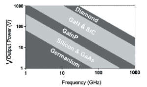
Fig. 1 Output power achievable as a function of frequency of different material semiconductors for 1 Ohm impedance
Experiments
The NCD films [5] were grown on p-type <100> Si substrates by Micro Wave plasma enhanced Chemical Vapor Deposition (MW CVD) in the ellipsoidal cavity reactor Aixtron P6. Substrates were mechanically seeded in ultrasonic bath using 5 nm diamond powder for 40 minutes. The growth step was performed at constant methane concentration (1% CH4 in H2) and the total gas pressure of 3 kPa. The total microwave power was 900 W and substrate temperature was 860 °C. Before contacting, the diamond layers were cleaned in H2SO4 + KNO3 solution with 10:1 ratio at 200 °C for 1 h. Contacts used for I–V measurements were formed by standard lithographic process by lift-off technique using the combination of Ti/Pt/Au materials with various thicknesses deposited by RF sputtering (Tab. 2).
| Ti thickness [nm] | Pt thickness [nm] | Au thickness [nm] | |
|---|---|---|---|
| 1 | 50 | 50 | 100 |
| 2 | 50 | - | 100 |
| 5 | 25 | 50 | 100 |
| 4 | 25 | - | 100 |
| 5 | - | 50 | 100 |
Tab. 2 Types of metal contacts used in experiments
Micro-Raman measurements of NCD were performed by using an ISA Dilor-Jobin Yvon-Spex Labram confocal system with 632.8 nm radiation from a He–Ne laser. Current–voltage characteristics were performed by a typical measurement set up in top–bottom contact arrangement showed in (Fig. 2).
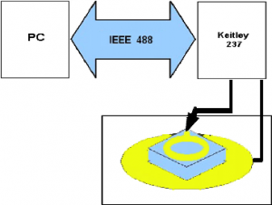
Fig. 2 Schema of I–V measurement set up
Main results
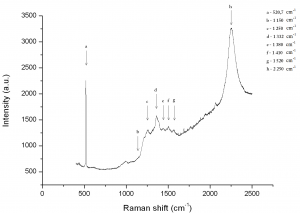
The quality of NCD films was determined from Raman spectra (Fig. 3). Measured Raman spectra consist of several bands: dominant Si peak is shown at 520.7 cm-1, a weak band related to small size nanodiamond crystals at about 1 150 cm–1, a weak band at 1 332 cm-1 is known as diamond peak and it is related to sp3 bonds, the sp2 graphitic phases are visible at 1 520 and 1 600 cm-1, then there is a broad band centered at 1 250 cm-1 related to CxHy [6,7] and a broad band of luminescence at 2 250 cm-1.
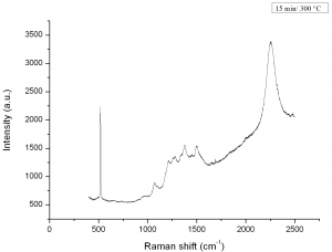
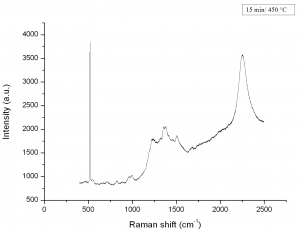
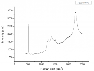
Fig. 3 The Raman spectra of the NCD thin film before and after annealing
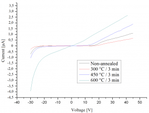
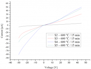
Raman spectra show that annealing caused changes in a structure mainly for various C-H bonds obtained in NCD thin film. Some C-H bonds almost get lost and typically diamond bonds stabilize. Electrical properties of samples were investigated by measuring of their I–V behaviors (Fig. 4, 5).
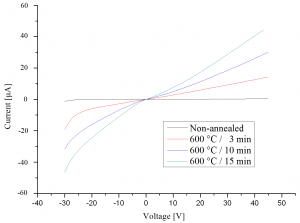
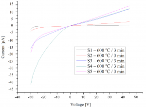
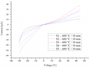
The behaviors of I–V measurements after high temperature annealing show ohmic (non-rectifying) character of the metal-NCD-Si sandwich structure. Fig. 5 shows current-voltage (I-V) characteristics before and after annealing of the sample depending on annealing temperature and/or on time of annealing. Figure 5 shows I-V characteristics of five different contact schemes prior to annealing at different times.
Fig. 4 I-V characteristics of as-deposited metal contacts on NCD samples measured before and after annealing
Fig. 5 I-V characteristics of as-deposited metal contacts on NCD samples measured after annealing of various lengths
From I–V measurements, we have found that there is a strong influence of annealing on electrical properties of our sandwich structure both in forward and reverse direction. This effect appears in the resistivity. The more sp2 bonds in the NCD film means more free electrons and thus the higher film conductivity for thinner NCD layers. Annealing at higher temperature and also for a longer period has a considerable effect to I-V characteristics and attaining higher current values in both directions.
Conclusions
In this study, we showed the influence of annealing of undoped NCD thin films and metal contacts on electrical properties of metal/NCD/Si sandwich structure. We can conclude that longer and more intensive annealing increases the current flow through the structure. Comparing accumulation and inverse region of current–voltage characteristics, ohmic (non-rectifying) contacts are detected. The influence of annealing to morphology of NCD thin film was confirmed by Raman spectroscopy, which is a very sensitive method to identify the sp3/sp2 ratio.
Acknowledgments
The authors would like to thank to Dr. A. Kromka (Institute of Physics, ASCRv.v.i., Czech Republic) for deposition of NCD samples and for valuable advice and to J. Král for technical support. This work was done in Center of Excelence CENAMOST (Slovak Research and Development Agency Contract No. VVCE-0049-07) with support of projects APVV-0628-06, APVV-0548-07, VEGA 1/3034/06, 1/0857/08, LPP-0246-06.
References
- Ch.J.H. Wort, R.S. Balmer, Diamond as an electronic material, Mater. Today 11 (1–2) (2008) 22–28
- Y.G. Chen, et al., Diamond Relat. Mater. 13 (2004) 2121–2124
- J.F. Prins, J. Phys. D: Appl. Phys. 22 (1989), p. 1562. View Record in Scopus | Cited By in Scopus (27)
- Y.G. Chen, M. Hasegawa, H. Okushi, S. Koizumi, H. Yoshida, T. Sakai and N. Kobayashi, Diamond Relat. Mater. 11 (2002), p. 451.
- S. Potocky, A. Kromka, J. Potmesil, Z. Remes, V. Vorlicek, M. Vanecek, M. Michalka, Diamond Relat. Mater. 16 (4–7) (2007) 744–747
- A.Kromka,J.Breza,M.Kadlecikova´ J.Janik, F.Balon, Carbon 43(2)(2005) 425–429
- S.Prawer, K.W.Nugent, D.N.Jamieson, J.O.Orwa, L.A. Bursill, J.L.Peng, Chem. Phys.Lett.332(2000)93–97
Co-authors of this paper are M.Vojs, M. Marton, P. Kubík, M. Veselý, Slovak University of Technology, Faculty of Electrical Engineering and Information Technology, Ilkovičova 3, 812 19 Bratislava.
