Synchronous rectifier in DC/DC converters
05. Október, 2009, Autor článku: Šaštinský Peter, Elektrotechnika, Študentské práce
Ročník 2, číslo 10  Pridať príspevok
 This paper is presented design of synchronous rectifiers for forward DC/DC converter of the switch-mode power supplies. Firstly are introduced different circuit diagrams of these rectifiers. Than are theoretically determined the limits of efficiency improvements that can be obtained by synchronous rectifiers. Finally are compared conversion efficiencies of control-driven SRs with those of different self-driven SR implementations. Specifically, performance comparisons of the forward converters with RCD-clamp and active-clamp reset are made.
Introduction
The conduction losses of diode rectifier contribute significantly to the overall power losses in a power supply, especially in low output-voltage applications [1]. The rectifier conduction losses are proportional to the product of its forward-voltage drop, VF, and the forward conduction current, IF.
Synchronous rectification (SR) is used in DC/DC converters when low output voltage is less than 5V and high current is needed [2]. Synchronous rectification utilizes power MOSFETs to rectify the output voltage of the power transformer. These MOSFETs are synchronized to the converter frequency and perform more efficiently the rectification of the output voltage than rectifying diodes due to the low I.R drop through the channel. The N channel power MOSFET offers the lowest ON resistance and is relatively inexpensive [4].
On the other hand, operating in the MOSFET III quadrant, a synchronous rectifier presents a resistive V-I characteristic, as shown in Fig. 1. Under certain current level, the forward-voltage drop of a synchronous rectifier can be lower than that of a diode rectifier, and consequently reduces the rectifier conduction losses. Due to the fact that synchronous rectifiers are active devices, the design and utilization of synchronous rectification need to be properly made.
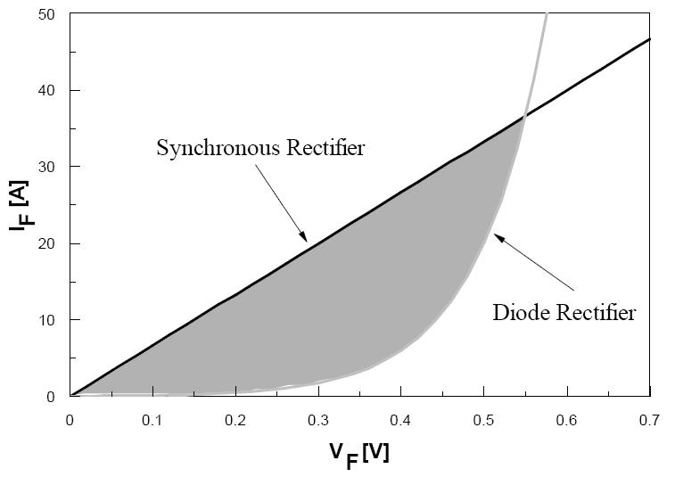
Fig. 1 Comparison of the forward voltage between diode rectifier and synchronous rectifier (gray area has conduction losses saving by using synchronous rectifiers)
Synchronous rectification in forward converter
A low-voltage plus high-current DC power supply is urgently required in the next-generation computer and communications equipment. The first idea is to use a forward converter, refer to Fig. 2, which can perform low-voltage plus high-current output voltage [1],[5]. The two diodes D1 and D2 can be normal rectifier diodes, rectifier Schottky diodes, or MOSFET transistors. Fig. 3 shows the efficiency gain of the following three types of forward converters needed to construct a low-voltage high-current power supply:
- Forward converter using traditional diodes
- Forward converter using Schottky diodes
- Synchronous rectifier using low forward-resistance MOSFET
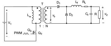
Fig. 2 Forward converter using traditional diodes
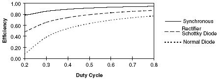
Fig. 3 Efficiencies of different types of forward converter
As the operating voltages increase, the design of rectifiers requires more attention because the devices forward-voltage drop constitutes an increasing fraction of the output voltage. The forward-voltage drop across a switch-mode rectifier is in series with the output voltage, so losses in this rectifier will almost entirely determine its efficiency. The synchronous rectifier circuit has been designed primarily to reduce these losses.
Circuit configurations
Based on the method employed in driving SRs, all of them can be classified into two groups: control-driven and self-driven. In a control-driven SR implementation, the SRs are driven by gate-drive signals derived from the gate-drive of the main switch. In a self-driven SR implementation, the SRs are driven directly with the secondary voltage of the transformer. As a result, the self-driven SR approach is very attractive since it is simple and requires a minimum number of components. However, the performance of self-driven SRs depends on the resetting method of the power transformer since the freewheeling synchronous rectifier is driven by the reset voltage. Ideally, it would be desirable that the resetting time be equal to the off-time of the primary switch. Then the output current would freewheel through the SR for the entire off (freewheeling) time.
Forward Converter with RCD-Clamp and Self-Driven SRs
The forward converter with self-driven SRs and its key waveforms are shown in Fig. 4 [3]. In this circuit, synchronous rectifiers SR3 (Q3 and D3) and SR4 (Q4 and D4) are crosscoupled to the secondary winding of the transformer and are directly driven by the secondary voltage. Since no driver or control circuit is used to provide the gate-drive signals, this implementation of synchronous rectification is the simplest possible. However, its performance is strongly dependent on the method of the transformer core resetting, because the gate-drive signal for synchronous rectifier SR4 is derived from the reset voltage.
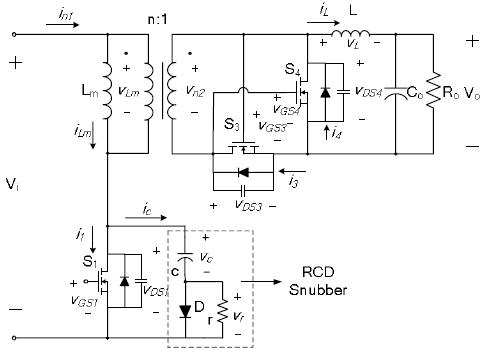
Fig. 4 Forward converter with RCD-clamp and self-driven SRs
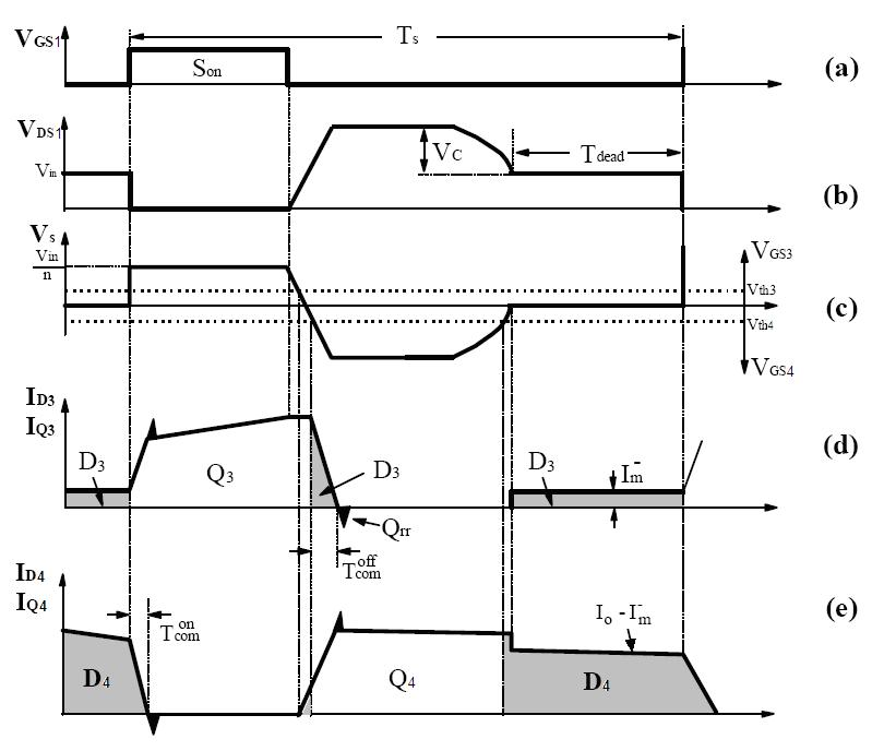
Fig. 5 Waveforms of a forward converter with RCD clamp and self-driven SRs: a) gate-drive signal, b) drain-to-source voltage of primary switch, c) secondary winding voltage, d) current through SR3 and e) current through SR4
As can be seen from the waveform in Fig. 5d, once the transformer reset is completed, the magnetizing current of the transformer, Im-, starts flowing through the body diode of SR2. The magnitude of this current is given by:
 |
(1) |
where N is the turns ratio of the transformer, VC is the transformer reset voltage, Lm is magnetizing inductance of the transformer, and CS is the total capacitance seen at the drain of the primary switch.
Also, as can be seen from the waveforms in Fig. 5e, after the transformer reset is completed, the difference between load current I0 and magnetizing current Im- is diverted from transistor Q4 to the body diode, D4, of SR4. Due to relatively high forward-voltage drops of the body diodes of SR3 and SR4, the efficiency of synchronous rectification is reduced. The efficiency losses due to the body-diode conduction depend on the duration of the dead time, Tdead, and the forward-voltage drops of the body diodes, VBD. These losses can be minimized by connecting Schottky diodes in parallel with SR3 and/or SR4 or by minimizing the conduction times of D3 and D4.
Forward Converter with Active Clamp and Self-Driven SRs
The forward converter with active-clamp reset and its key waveforms are shown in Fig. 6 [3]. As can be seen, the active-clamp-reset approach minimizes the duration of the dead time since the transformer core is reset during almost the entire off time of the primary switch. As a result, the conduction time of transistor Q4 is maximized, the time during which D3 is conducting magnetizing current is minimized. Consequently, the conversion efficiency of the converter with the active-clamp reset is improved relative to the RCD-clamp counterpart.
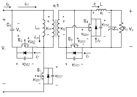
Fig. 6 Forward converter with active-clamp and self-driven SRs
Also, the active-clamp reset approach minimizes voltage stress on the primary switch. However, the active clamp approach requires an extra switch and its associated gate drive, compared to the same circuit with the RCD-clamp reset. From this perspective, it is much simpler and more economical to use a Schottky diode in parallel with SR3 to improve the efficiency of the RCD-clamp circuit than it is to implement the active clamp. Therefore, the active-clamp approach is a viable choice in synchronous-rectifier applications where voltage stress and soft-switching are important design considerations.
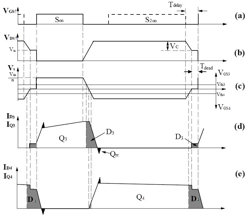
Fig. 7 Waveforms of a forward converter with active-clamp and self-driven SRs: a) gate-drive signals, b) drain-to-source voltage of primary switch, c) secondary winding voltage, d) current through SR3 and e) current through SR4
Forward Converter with RCD Clamp and Control-Driven SRs
The forward converter with control-driven SRs and its key waveforms are shown in Fig. 8 [3]. In this circuit, transistors Q3 and Q4 are driven by gate-drive signals derived from the primary-switch gate drive. As a result, the conduction times of the synchronous rectifiers are independent of the transformer-resetting method, but solely depend on the timing of the gate-drive signals. However, as can be seen from Figs. 9d and 9e, while driving the SRs from the control circuit results in the maximum conduction time of Q4, it has no effect on the conduction time of the magnetizing current though diode D3 during the dead time. Namely, since during the dead time transistor Q3 is off (gate-drive to Q3 is low), the conduction of diode D3 during the dead time with control-driven SRs (see Fig. 8 ) is exactly the same as for the self-driven SRs (see Fig. 4).

Fig. 8 Forward converter with RCD-clamp and control-driven SRs
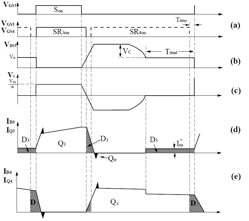
Fig. 9 Waveforms of a forward converter with RCD clamp and control-driven SRs: a) gate-drive signal, b) drain-to-source voltage of primary switch, c) secondary winding voltage, d) current through SR3 and e) current through SR4
Forward Converter with Active Clamp and Control-Driven SRs
The basic circuit configuration shown in Fig. 10 is similar to that shown in Fig. 6. The only difference is that the whole circuit in Fig. 10 is fully-controlled by the microcontroller.
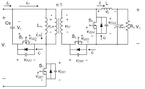
Fig. 10 Forward converter with active-clamp and control-driven SRs
In practical applications, this ideally complementary drive is not possible. The driving pulses are shown in Fig. 11. The dead times are included that will not occur brief overlapping of the gate-drive signals simultaneously that would short on the primary or the secondary, causing an increased primary or secondary current, and thus would lower efficiency or, in severe cases, would cause converter failure.
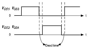
Fig. 11 Waveforms of driving pulses for forward converter with active-clamp and control-driven SRs
Efficiency limits of synchronous rectification
The efficiency improvement that can be achieved by replacing Schottky rectifiers with SRs is a complex function of many parameters. The most important are the output voltage, output current, SR on-resistance, forward-voltage drop of Schottkies that are being replaced by SRs, the transformer resetting method, efficiency of the converter with Schottkies, and implementation of SRs (i.e., with or without Schottkies in parallel with SRs). Generally, the efficiency of a converter can be expressed as
 |
(2) |
where P0 is the output power, Ploss are the total losses excluding the rectifier losses, and PREC are the rectifier losses. For a converter with Schottky rectifiers, the efficiency is
 |
(3) |
Similarly, for the same converter with SRs, the efficiency is
 |
(4) |
Eliminating Ploss from the above equations, the efficiency of the converter with SRs, 

 |
(5) |
The power losses in the Schottky rectifiers can be calculated as
 |
(6) |
where VSH is the forward-voltage drop of the Schottkies, and I0 is the output current. The power losses of the self-driven SRs, PSRsd, for both RCD-and active-clamp reset are given by:
}I_{0}^{2}(1-D_{dead})+V_{D}I_{0}D_{dead}+P_{gate}+P_{PREC}") |
(7) |
where RDS(on) is the on-resistance of SRs, Ddead = Tdead/Ts is the dead-time duty cycle, VD is the forward-voltage drop of the antiparallel diodes across SR3 and SR4, Pgate are the gate-driven losses, and PRREC are the power losses associated with the reverse-recovery of the body diodes of the SRs. It should be noted that Eq. 7 is derived assuming that commutation times Tcom on and Tcomoff are zero, that synchronous rectifiers SR3 and SR4 have identical on resistance (RDS(on)3 = RDS(on)4 = RDS(on)), and that diodes D3 and D4 have identical voltage drops (VD3 = VD4 = VD) which are independent of their currents.
For self-driven SRs with active-clamp reset, the dead time is very short relative to a switching period, and therefore, Ddead >> 0. However, for the converter with the self-driven SRs and with the RCD-clamp reset, this duty cycle usually cannot be neglected. In this case, the losses depend on the duration of the dead time and VD of the antiparallel diodes of the SRs. Generally, these diodes can be the body diodes of SRs (VD = VBD) or externally added Schottkies in parallel with SRs (VD = VSH). The power loss of the control-driven SRs is given by:
}I_{0}^{2}(1-D_{dead})+R_{DS(on)}(I_{0}-I_{m}^{-})^2(D_{dead}-D_{delay})") |
(8) |
D_{delay}+P_{gate}+P_{PREC}") |
where Ddelay = Tdelay/Ts is the delay-time duty cycle, and Tdelay is the delay time between the SR4 gate-drive turn-off and SR3 gate-drive turn-on as indicated in Fig. 6b. The gate-drive losses, Pgate, are a function of the gate-to-source voltage of SR, frequency, and gate charge required to charge SRs’ capacitance to the gate-source voltage. A method of estimating these losses for self-driven SRs was presented in [5]. For control-driven SRs these losses are higher since it includes also the losses in the external drivers and their associated logic.
The reverse-recovery losses, PRREC, are only presented in implementations where the body diode of the SR is conduction (no Schottky in parallel with SR). When the gate-drive losses and the reverse-recovery losses are neglected (Pgate = PRREC << 0), the efficiency of the forward converter with the self-driven SRs for both RCD- and active-clamp implementations is
![\frac{1}{\eta_{SR}^{sd}} = \frac{1}{\eta_{SH}}-\frac{V_{SH}}{V_{0}} \left [ 1-\frac{R_{DS(on)}I_{0}}{V_{SH}}(1-D_{dead})-\frac{V_{D}}{V_{SH}}D_{dead} \right ]](https://s0.wp.com/latex.php?latex=%5Cfrac%7B1%7D%7B%5Ceta_%7BSR%7D%5E%7Bsd%7D%7D+%3D+%5Cfrac%7B1%7D%7B%5Ceta_%7BSH%7D%7D-%5Cfrac%7BV_%7BSH%7D%7D%7BV_%7B0%7D%7D+%5Cleft+%5B+1-%5Cfrac%7BR_%7BDS%28on%29%7DI_%7B0%7D%7D%7BV_%7BSH%7D%7D%281-D_%7Bdead%7D%29-%5Cfrac%7BV_%7BD%7D%7D%7BV_%7BSH%7D%7DD_%7Bdead%7D+%5Cright+%5D&bg=ffffff&fg=000000&s=1 "\frac{1}{\eta_{SR}^{sd}} = \frac{1}{\eta_{SH}}-\frac{V_{SH}}{V_{0}} \left [ 1-\frac{R_{DS(on)}I_{0}}{V_{SH}}(1-D_{dead})-\frac{V_{D}}{V_{SH}}D_{dead} \right ]") |
(9) |
Since for the forward converter with self-driven SRs and active-clamp reset (D
![\frac{1}{\eta_{SR}^{acl}} = \frac{1}{\eta_{SH}}-\frac{V_{SH}}{V_{0}} \left [ 1-\frac{R_{DS(on)}I_{0}}{V_{SH}} \right ]](https://s0.wp.com/latex.php?latex=%5Cfrac%7B1%7D%7B%5Ceta_%7BSR%7D%5E%7Bacl%7D%7D+%3D+%5Cfrac%7B1%7D%7B%5Ceta_%7BSH%7D%7D-%5Cfrac%7BV_%7BSH%7D%7D%7BV_%7B0%7D%7D+%5Cleft+%5B+1-%5Cfrac%7BR_%7BDS%28on%29%7DI_%7B0%7D%7D%7BV_%7BSH%7D%7D+%5Cright+%5D&bg=ffffff&fg=000000&s=1 "\frac{1}{\eta_{SR}^{acl}} = \frac{1}{\eta_{SH}}-\frac{V_{SH}}{V_{0}} \left [ 1-\frac{R_{DS(on)}I_{0}}{V_{SH}} \right ]") |
(10) |
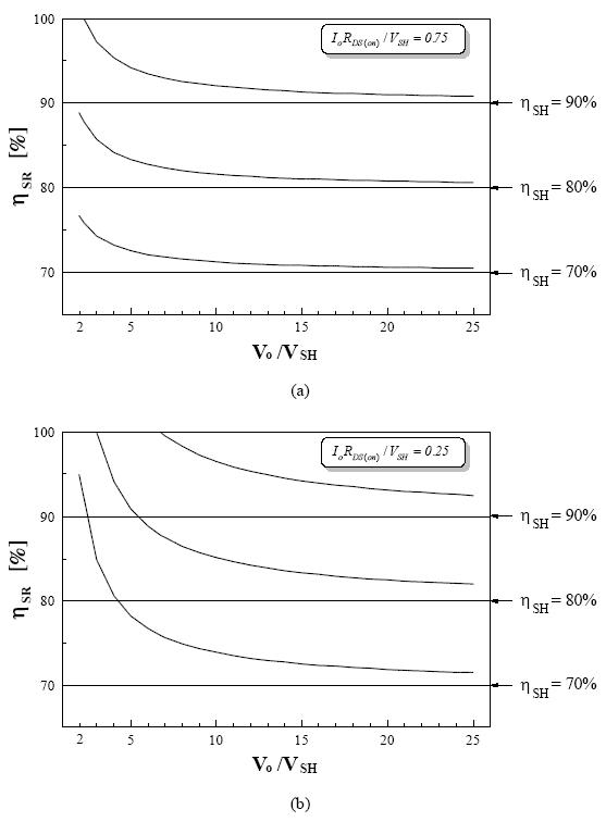
Fig. 12 Efficiency limits of forward converter with self-driven SRs and active-clamp reset and control-driven SRs with small gate-drive timing delay (Ddelay >> 0) and magnetizing current Im- << I0: a) α = RDS(on)·I0/VSH = 0,75, and b) α = 0,25
Eqs. 9 and 10 can be regarded as the best-case efficiency limits of different SR implementations. The efficiencies of the forward converter with control-driven SRs, 
}I_{0}}{V_{SH}}(1-D_{dead})") |
(11) |
}I_{0}}{V_{SH}} \left ( 1-\frac{I_{m}^{-}}{I_{0}} \right )^2 (D_{dead}-D_{delay})") |
|
![-\frac{V_{D}I_{m}^{-}}{V_{SH}I_{0}} D_{dead}-\frac{V_{D}}{V_{SH}} \left ( 1-\frac{I_{m}^{-}}{I_{0}} \right ) D_{delay}]](https://s0.wp.com/latex.php?latex=-%5Cfrac%7BV_%7BD%7DI_%7Bm%7D%5E%7B-%7D%7D%7BV_%7BSH%7DI_%7B0%7D%7D+D_%7Bdead%7D-%5Cfrac%7BV_%7BD%7D%7D%7BV_%7BSH%7D%7D+%5Cleft+%28+1-%5Cfrac%7BI_%7Bm%7D%5E%7B-%7D%7D%7BI_%7B0%7D%7D+%5Cright+%29+D_%7Bdelay%7D%5D&bg=ffffff&fg=000000&s=1 "-\frac{V_{D}I_{m}^{-}}{V_{SH}I_{0}} D_{dead}-\frac{V_{D}}{V_{SH}} \left ( 1-\frac{I_{m}^{-}}{I_{0}} \right ) D_{delay}]") |
If magnetizing current Im- << I0 so that its losses can be neglected, and if the delay time is short so that Ddelay >> 0, Eq. 11 simplifies to Eq. 10. Fig. 12 shows the plots of this equation. These plots present the efficiency of a converter with SRs, 
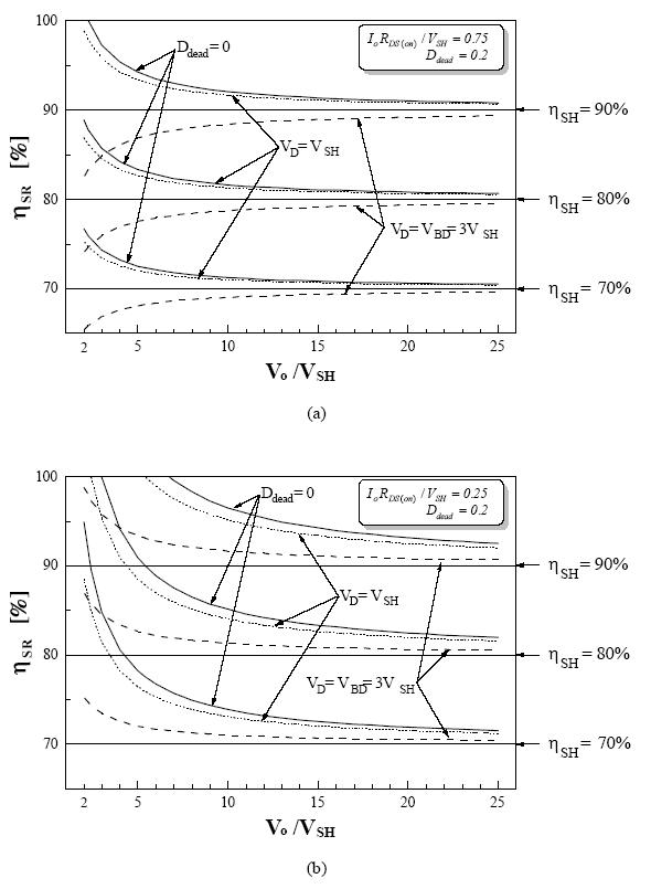
Fig. 13 Efficiency limits of forward converter with self-driven SRs and RCD-clamp reset for Ddead = 0,2: a) α = RDS(on)·I0/VSH = 0,75, and b) α = 0,25
As can be seen, the efficiency improvement for a given α and a given VSH is lower at higher output voltages, V0. Also, for the same output voltage, the efficiency gain achieved by synchronous rectification is higher for converters with higher efficiencies with Schottky diodes,
Conclusion
In this paper was presented design of synchronous rectifiers for forward DC/DC converter. There were introduced control-driven and self-driven circuit diagrams of these rectifiers. The limits of efficiency improvements that can be obtained by synchronous rectifiers are primarily a function of the output voltage, output current, on-resistance of the SR, and the forward-voltage drop of Schottky rectifiers replaced by SRs. In the end, performance comparisons of the forward converters with RCD-clamp and active-clamp reset were made.
References
- Zhang M. T., “Electrical, thermal, and EMI designs of high-density, low-profile power supplies,” Dissertation, Faculty of the Virginia Polytechnic Institute, 1997 Blacksburg, Virginia.
- Luo L. F., Ye H., “Advanced DC/DC Converters”, CRC Press LLC, Boca Raton 2004, ISBN 0-8493-1956-0
- Jinno M., Chen P. Y., Shie Y. M., “Study on the reverse conduction of synchronous rectifiers,” 2006 IEEE Region 10 Conference, Tencon 2006, pp. 1-4.
- Beta-Dyne, Application Note DC-006, DC/DC Converters: Synchronous rectification
http://www.beta-dyne.com/pdf/dcdc_an6_rev01.pdf - Blanc J., “Practical application of MOSFET synchronous rectifiers,” Proc. IEEE Int. Telecommun. Energy Conf., 1991, pp. 495-501.
- Hribik J., Hruškovic M., “Power Supply Source for Class TD Power Amplifiers,” In: Proceedings of the 17th Internacional Czech-Slovak Scientific Conference “Radioelektronika 2007”, Brno (Czech Republic), 2007, pp.105-108.
Co-author of this paper is M. Jendruch, Slovak University of Technology, Faculty of Electrical Engineering and Information Technology, Ilkovičova 3, 812 19 Bratislava.