Modeling of a robust pressure sensor based on progressive semiconductor materials
11. November, 2013, Autor článku: Vincze Tamás, Elektrotechnika
Ročník 6, číslo 11  Pridať príspevok
![]() This work deals with modeling and analysis of a micro electro mechanical pressure sensor based on a piezoelectric membrane with high electron mobility AlGaN/GaN heterostructure transistors (HEMT). The results of the static piezoelectric analysis are shown. The differences in the curves of the produced electric field intensities and the charge changes of the gate electrodes at different values of pressure are monitored. As a result of this modeling, different types of simulations were carried out and analyzed.
This work deals with modeling and analysis of a micro electro mechanical pressure sensor based on a piezoelectric membrane with high electron mobility AlGaN/GaN heterostructure transistors (HEMT). The results of the static piezoelectric analysis are shown. The differences in the curves of the produced electric field intensities and the charge changes of the gate electrodes at different values of pressure are monitored. As a result of this modeling, different types of simulations were carried out and analyzed.
1. Introduction
A micro electro mechanical system (MEMS) is a term describing a device with micro dimensions, which consist of a combination of electrical and mechanical components. It is used as a sensor or an actuator and allows a subsequent evaluation and processing of the measured data [1]. III – nitride semiconductor materials are characterized by a high mechanical and thermal stability and large piezoelectric coefficients. Thanks to this unique set of properties, these materials have great potential for use in micro electro mechanical systems, especially for extreme conditions [2][3]. They withstand higher temperatures, mechanical stress and also chemically aggressive environments.
2. The AlGaN/GaN heterostructure
A semiconductor heterostructure or in other words a semiconductor heterojunction is created by epitaxial technology, and it is defined as a structure of materials with unequal band gap widths [4]. GaN is a binary compound of III – nitrides which exhibits a spontaneous polarization. Moreover it has a high chemical resistance and mechanical strength, which is preserved in a wide temperature range. The increase of the Al content in the epitaxial growth of GaN (Ga atoms are replaced by Al atoms) arises a ternary compound AlxGax-1N (x represents the molar content of Al) with different band gap widths. The aluminum content plays also a big role in the increase of overall structure polarization. The AlGaN/GaN heterostructure is defined as a combination of these two materials [5].
After connecting a wide and a narrow band gap semiconductor, inequality arises between the conduction band ΔEC and the valence band ΔEV. This inequality causes the bending of energy bands at the interface, thereby creating a two-dimensional conducting channel (2DEG) Fig.2.1. [4]
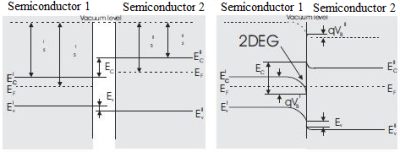
Fig.2.1. Energy bands at the interface of heterostructure [4]
Spontaneous and piezoelectric polarization in materials GaN and AlN is more than ten times larger than in conventional III – V and II – VI semiconductor compounds [6]. In case of III – V nitrides, the total polarization by given deformation, zero temperature and the absence of external electric field can be described by the equation
| (2.1) |
where PSP represents the spontaneous polarization in the material and PPZ(ε) is the piezoelectric polarization at a given deformation. Spontaneous polarization has a fixed direction (0001) in the crystal structure, but the piezoelectric polarization may occur in any direction depending on the direction of loading. The polarization charge at the interface can arise from two sources: from piezoelectric effect in a stressed AlGaN layer and from the difference of spontaneous polarization between GaN and AlGaN. [4]
If the result of total polarization is a positive charge, electrons start to move from a wider band gap material (AlGaN layer) to the narrow one (GaN layer) and creates a two-dimensional electron gas with a high concentration and high charge carrier mobility at the interface. Thanks to this feature the AlGaN/GaN heterostructure is suitable for piezoelectric applications. [7]
3. High Electron Mobility Transistors
The mentioned multilayer structures, thus the semiconductor structures and the two-dimensional electron gas are key fundamentals of high electron mobility transistors, also called HEMTs. Final HEMT structures are created via three electrodes, (source, gate, drain) which are formed on the top surface of the AlGaN layer by Schottky and ohmic contacts shown on Fig.3.1. The current between the source and drain contacts is controlled by space charge, which is adjusted by the input voltage on the gate electrode. By a suitable applied voltage, current flows through the conductive channel formed by 2DEG, hence the channel conductance depends on the concentration and mobility of the charge carriers.
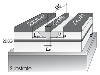
Fig.3.1. Schematic model of a HEMT structure [4]
4. Structure of the sensor
The structure of the sensor is based on a circle shaped membrane heterostructure model, created on a SiC substrate attached to a steel case from the bottom by fritted glass Fig.4.1. The main dimensions are: ϕ = 8mm, A = 0.1mm, B = 2mm. Thicknesses of individual layers of the membrane are: steel = 100 μm, fritted glass = 100μm, SiC = 350μm, GaN = 2.85μm, AlGaN = 20nm. The model of the sensor and all the simulations were realized using the software Ansys.
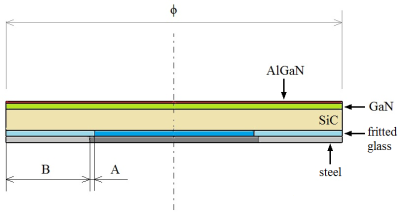
Fig.4.1.SiC substrate and structure of the AlGaN/GaN sensor
The sensors, thus the sensing HEMT transistors are placed at specific locations on the top of the AlGaN layer according to Fig.4.2. Locations of these transistors depend on the expected distribution of the electric field along the membrane.
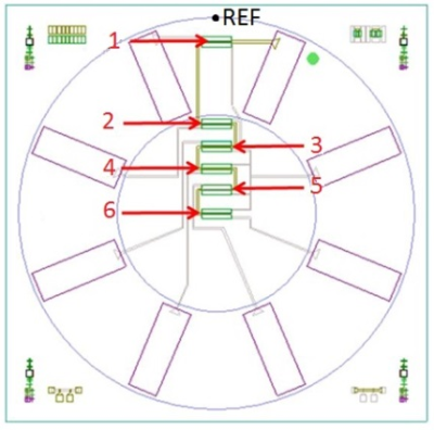
Fig.4.2. Layout of the HEMT transistors along the multilayer membrane [8]
Dimensions of these transistors are summarized in Tab.4.1. In the final model, the AlGaN layer is located only under individual transistors, elsewhere it is removed by etching during production.
Tab.4.1.Location of transistors from the reference point
| Width of gate | Distance from the reference point (REF) [μm] | |||||
|---|---|---|---|---|---|---|
| Lg [μm] | 1 | 2 | 3 | 4 | 5 | 6 |
| 10 | 500 | 2180 | 2635 | 3090 | 3520 | 4000 |
5. Constitutive equations of the piezoelectric effect
The basis of the piezoelectric effect is Hooke´s law and the constitutive equation of electrostatic field. Hooke´s law defines the relation between mechanical deformation and mechanical stress of the material, and has the following form
| (5.1) |
where σij represents components of the mechanical stress tensor, Cijkl represents components of the elastic tensor of the material and εkl describes components of the mechanical strain tensor. The constitutive equation of electrostatic field describes the electrical properties of the material, and is defined as:
| (5.2) |
where Di defines components of the electric displacement vector, ϵik describes components of the electric permittivity tensor and Ek represents components of the electric field intensity vector. By combining these two we get:
| (5.3) |
| (5.4) |
where CijklE defines components of the tensor of elastic properties of the material in a state of constant electric field, ϵikε describes components of electric permittivity tensor at constant mechanical strain and eikl corresponds to components of the piezoelectric module tensor, which appears in both equations representing a connection between mechanical stress and electric field. If eikl = 0, the connection is canceled and the equations are reduced to Hooke´s law and the equation for the electrostatic field. If eikl ≠ 0, and when the material is exposed to deformation, the electric displacement, thus the polarization can take a nonzero value at a zero electric field. The opposite is also true, which means that the electric field may cause material deformation in the case of the absence of mechanical stress.
Di and Ek are vectors with 3 components. Due to the symmetry of mechanical stress and mechanical strain tensors, σq and εq are reduced to vectors with 6 elements. CpqE and SpqE are matrixes 6×6, epk and diq have dimension of 3×6 and the matrix ϵikε has a 3×3 dimension. Used materials GaN, AlGaN and SiC are transversally isotropic materials, what means that there is a symmetry axis and the plane perpendicular to it – isotropic plane in which the material properties are same in any direction. Thanks to that, the total number of elastic constants is reduced to 5 and the number of piezoelectric coefficients to 3. The matrix form of the constitutive equations is defined as:
The used material properties are shown in the following tables:
Tab.5.1.Mechanical material properties
| Layer | Elastic coefficients | Density | ||||
|---|---|---|---|---|---|---|
| C11 [GPa] | C12 [GPa] | C13 [GPa] | C33 [GPa] | C44 [GPa] | ρ [kg/m3] | |
| SiC | 501 | 111 | 52 | 553 | 163 | 3211 |
| GaN | 390 | 145 | 103 | 405 | 105 | 6150 |
| AlGaN | 395 | 146 | 104,25 | 386,25 | 110 | 5190 |
Steel and glass are isotropic materials, their properties are defined by Young´s modulus and Poisson´s ratio. Material properties of isotropic materials are shown in Tab.5.2.
Tab.5.2.Material properties of isotropic materials
| Layer | Young´s modulus | Poisson´s ratio | Density |
|---|---|---|---|
| E [GPa] | - | ρ [kg/m3] | |
| glass | 60 | 0,3 | 2800 |
| steel | 210 | 0,3 | 8100 |
Values of the piezoelectric coefficients are defined in Tab.5.3.
Tab.5.3.Piezoelectric coefficients
| Layer | Piezoelectric coefficients | Rel. permittivity | ||
|---|---|---|---|---|
| e13 [C/m2] | e33 [C/m2] | e15 [C/m2] | εr [F/m] | |
| GaN | -0,36 | 1 | -0,3 | 8.9 |
| AlGaN | -0,51 | 0,67 | 0,375 | 8.9 |
6. Investigation of the electric field intensity on the proposed sensor
Initial analysis included the electric field investigation on the membrane surface. Due to symmetry of the sensor we were able to create quarter models of the membrane and define the symmetric boundary conditions, thereby a simplified simulation. To get a continuous curve of the electric field intensity, the upper surface of AlGaN was modeled as a continuous surface – see Fig.6.1.
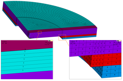
Fig.6.1. Quarter model of sensor with detail view of the used materials: 1 – GaN, 2 – SiC, 3 – glass, 4 – steel, 5 –AlGaN
It should be mentioned here that the electrical degree of freedom in the lower surface of AlGaN layer was coupled. This represents the bottom electrode of the piezoelectric material, which was grounded. The following steps were realized: definition of symmetric boundary conditions, fixation of the model at the bottom of the steel layer, definition of the static pressure on the top surface of the sensor and investigation of the electric field intensity on the top surface of the AlGaN layer. The pressure was varied from 1 to 3 MPa. Curves and the character of the electric field intensities are shown on Fig.6.2. There are also indicated the positions of transistors along the membrane.
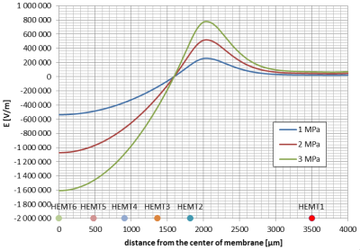
Fig.6.2.Character of electric field intensities at different values of pressure
We can notice here that the resulting electric field intensities increase with the increasing pressure. Middle of the membrane indicates 0 microns. The intensity has a negative value around the center of the membrane and a positive value at the fixed region (around 2000 μm). This is due to the fact that the piezoelectric material is compressed form the center of the membrane to 1600μm. The rest of the membrane is stretched.
7. Effects of substrate material etching
The next task was to investigate the influence of the substrate material modification by etching procedure on the sensor’s sensitivity. We modified the top AlGaN layer according to the real sensor, thus we modeled this layer only under the individual transistors. We also created electrodes on the top surface of the sensor, thus the gate electrodes of these transistors. On Fig.7.1. we see the modified model with the realized gate electrodes and with 50 μm depth etching of the substrate material. The etching procedure generates rounded edges according to Fig.7.1. with a considered constant radius 10 μm.
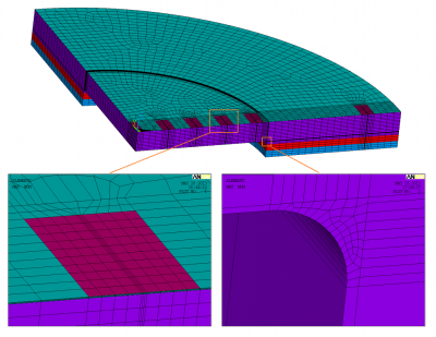
Fig.7.1. Modified model of the sensor with detail view of one transistor and radius
After evaluating the model, the most sensitive place was at the rounded edges. This area shoved the most stressed location of the model Fig.7.2.
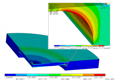
Fig.7.2. Layout of mechanical stress (in MPa) at pressure 3 MPa and etching 150 μm on the whole model and at the area of rounded edges
We had to determine the maximum pressure that the system can withstand at given depths of the etching, therefore we varied the magnitude of the pressure at each etching level and we noted the value of the maximum mechanical stress. Obtained graphs are shown on Fig.7.3.
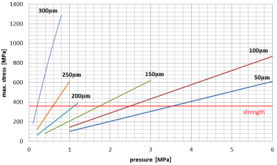
Fig.7.3. Function of maximum stress by the magnitude of pressure. Indicated numbers represent the etching levels.
Maximum pressure values are shown in Tab.7.1
Tab.7.1. Values of the calculated maximum pressures for the individual levels of etching
| Etching [μm] | Regression equation | Max. pressure [MPa] |
|---|---|---|
| 50 | y = 102.06x + 0.232 | 3.525 |
| 100 | y = 144.76x + 0.1924 | 2.486 |
| 150 | y = 207.27x + 0.5664 | 1.734 |
| 200 | y = 323.81x + 0.5915 | 1.11 |
| 250 | y = 611.73x + 1.348 | 0.586 |
| 300 | y = 1589.8x + 39.925 | 0.201 |
The strength of the substrate material was set to 360 MPa according to the literature [9]. This limit is indicated by the red line sown on the Fig.7.3. Using linear regression, the maximum pressure what the system withstands at certain etching level was defined. Simulations followed were realized by the loading of the sensor in accordance to the obtained range of pressure. We considered also the effect of the residual stress, which occurs during production. This value was defined by the reference [10] as 183 MPa a tensile stress in the x and y direction. The change of electric charge on the gate electrodes of transistors for different etching levels and for different loads was monitored. Transistors are marked according to Fig.4.2.
Transistor labeled as HEMT1 is a reference structure, etching the substrate material has no effect on this transistor. Transistor HEMT2 is located near the border of the fixed region. The dependence of the electric charge on the pressure magnitude is shown on Fig.7.4. Piezoelectric material is stretched with the result of a positive charge on the electrode.
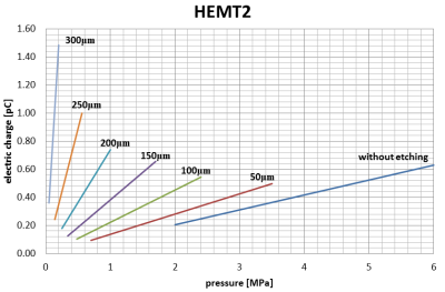
Fig.7.4. Electric charge of the transistor HEMT2 at different etching levels
Other transistors are placed in a row on the membrane according to Fig.4.2., where the piezoelectric material is compressed by pressure. Compression causes piezoelectric polarization of opposite polarity. In comparison with the transistor HEMT2, these transistors evoke negative charge, what is shown on Fig.7.5.
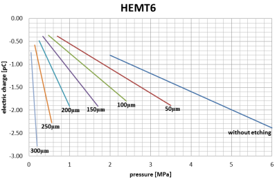
Fig.7.5. Electric charge on transistor HEMT6 at different etching level
Fig.7.6. shows the total mechanical strain in the z direction in the material GaN and AlGaN at 6 MPa pressure without etching. As illustrated, at the bending point of the membrane negative mechanical strain was created. The material is compressed in the direction z. At the center of membrane positive mechanical strain was monitored, piezoelectric material is stretched in the z direction. The polarity of the charge generated on the gate electrodes of the transistors depends on the mechanical strain.
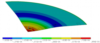
Fig.7.6. Total mechanical strain in direction z in material GaN and AlGaN at 6MPa pressure
Comparison of the electric charge on the gate electrodes of transistors without and at 300μm etching is illustrated on following figures.
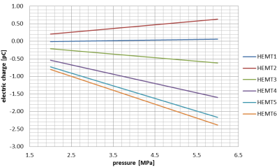
Fig.7.7. Electric charge differences on gate electrodes of all transistors without etching
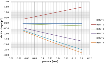
Fig.7.8. Electric charge differences on gate electrodes of all transistors with 300μm etching
The slope of the individual curves describes the sensitivity of these transistors. It provides information about how electric charge changes depending on the pressure change. Fig.7.9. shows how the level of etching affects the sensitivity of the transistors.
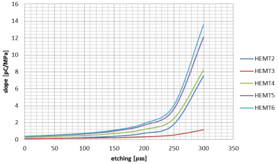
Fig.7.9. The dependence of the transistors sensitivity on the etching level
8. Effect of temperature rise
We investigated the effect of temperature on the electric charge of the transistor HEMT6, which appeared in the previous simulations as the most sensitive. We defined a uniform temperature on the whole model. The reference temperature was 300K. We had to define the temperature-dependent material properties of individual materials according to the following tables.
Tab.8.1 Temperature dependent material properties of GaN [11] [12]
| GaN | ||||||
|---|---|---|---|---|---|---|
| Properties | T [K] | 400 | 500 | 600 | 700 | 800 |
| t [°C] | 126.85 | 226.85 | 326.85 | 426.85 | 526.85 | |
| Elastic coefficients | C11 [GPa] | 372.6 | 370.7 | 368.5 | 366.3 | 364.1 |
| C12 [GPa] | 140.6 | 139.8 | 138.8 | 137.7 | 136.7 | |
| C13 [GPa] | 97.4 | 96.7 | 96 | 95.3 | 94.5 | |
| C33 [GPa] | 382.3 | 380 | 377.8 | 375.5 | 373.3 | |
| C44 [GPa] | 98.1 | 97.9 | 97.7 | 97.5 | 97.3 | |
| C66 [GPa] | 116 | 115.45 | 114.85 | 114.3 | 113.7 | |
| Thermal conductivity | λ [W/mK] | 155.77 | 119.18 | 95.761 | 79.59 | 67.80 |
| Thermal expansion | αa [10-6 K-1] | 4.55 | 4.89 | 5.10 | 5.24 | 5.34 |
| αc [10-6 K-1] | 4.05 | 4.33 | 4.49 | 4.59 | 4.66 | |
Tab.8.2.Temperature dependent material properties of AlN [12] [13] [14]
| AlN | ||||||
|---|---|---|---|---|---|---|
| Properties | T [K] | 400 | 500 | 600 | 700 | 800 |
| t [°C] | 126.85 | 226.85 | 326.85 | 426.85 | 526.85 | |
| Elastic coefficients | C11 [GPa] | 407.08 | 405.7 | 404.32 | 402.83 | 401.2 |
| C12 [GPa] | 99.94 | 99.6 | 99.26 | 98.9 | 98.51 | |
| C13 [GPa] | 83.2 | 82.92 | 82.64 | 82.34 | 82.01 | |
| C33 [GPa] | 383.4 | 382.1 | 380.8 | 379.4 | 377.9 | |
| C44 [GPa] | 99.84 | 99.51 | 99.17 | 98.8 | 98.41 | |
| C66 [GPa] | 153.57 | 153.05 | 152.53 | 151.97 | 151.35 | |
| Thermal conductivity | λ [W/mK] | 214.62 | 146.87 | 107.72 | 82.89 | 66.06 |
| Thermal expansion | αa [10-6 K-1] | 3.98 | 4.73 | 5.30 | 5.73 | 6.06 |
| αc [10-6 K-1] | 3.09 | 3.80 | 4.36 | 4.78 | 5.09 | |
Material properties of AlGaN were calculated using Vegard´s law according to the formula (8.1), where x represents the molar content of Al in the AlGaN compound, in our case x=0,25.
| (8.1) |
Tab.8.3.Temperature dependent material properties of AlGaN
| AlGaN | ||||||
|---|---|---|---|---|---|---|
| Properties | T [K] | 400 | 500 | 600 | 700 | 800 |
| t [°C] | 126.85 | 226.85 | 326.85 | 426.85 | 526.85 | |
| Elastic coefficients | C11 [GPa] | 381.22 | 379.45 | 377.46 | 375.43 | 373.38 |
| C12 [GPa] | 130.44 | 129.75 | 128.92 | 128 | 127.15 | |
| C13 [GPa] | 93.85 | 93.26 | 92.66 | 92.06 | 91.38 | |
| C33 [GPa] | 382.58 | 380.53 | 378.55 | 376.48 | 374.45 | |
| C44 [GPa] | 98.54 | 98.30 | 98.07 | 97.83 | 97.58 | |
| C66 [GPa] | 125.39 | 124.85 | 124.27 | 123.72 | 123.11 | |
| Thermal conductivity | λ [W/mK] | 170.49 | 126.10 | 98.75 | 80.41 | 67.37 |
| Thermal expansion | αa [10-6 K-1] | 4.41 | 4.85 | 5.15 | 5.36 | 5.52 |
| αc [10-6 K-1] | 3.81 | 4.20 | 4.46 | 4.64 | 4.77 | |
We considered material SiC as an isotropic material. Its material properties are summarized in Tab.8.4.
Tab.8.4. Temperature dependent material properties of SiC [9]
| SiC | ||||||
|---|---|---|---|---|---|---|
| Properties | T [K] | 400 | 500 | 600 | 700 | 800 |
| t [°C] | 126.85 | 226.85 | 326.85 | 426.85 | 526.85 | |
| Young´s modulus | E[GPa] | 412.08 | 409.78 | 407.48 | 405.18 | 402.88 |
| Poisson´s ratio | v [-] | 0.159 | 0.159 | 0.159 | 0.159 | 0.160 |
| Thermal conductivity | λ [W/mK] | 92.08 | 78.11 | 67.80 | 59.88 | 53.60 |
| Thermal expansion | α [10-6 K-1] | 2.32 | 2.97 | 3.32 | 3.49 | 3.56 |
For the glass we consider the Yung´s modulus and Poisson´s ratio as constant.
Tab.8.5.Temperature dependent material properties of glass [15]
| glass | ||||||
|---|---|---|---|---|---|---|
| Properties | T [K] | 400 | 500 | 600 | 700 | 800 |
| t [°C] | 126.85 | 226.85 | 326.85 | 426.85 | 526.85 | |
| Young´s modulus | E[GPa] | 60 | 60 | 60 | 60 | 60 |
| Poisson´s ratio | v [-] | 0,3 | 0,3 | 0,3 | 0,3 | 0,3 |
| Thermal conductivity | λ [W/mK] | 1.5 | 1.55 | 1.7 | 1.85 | 2.05 |
| Thermal expansion | α [10-6 K-1] | 0.53 | 0.59 | 0.59 | 0.57 | 0.55 |
Tab.8.6.Temperature dependent material properties of steel [16]
| steel | ||||||
|---|---|---|---|---|---|---|
| Properties | T [K] | 400 | 500 | 600 | 700 | 800 |
| t [°C] | 126.85 | 226.85 | 326.85 | 426.85 | 526.85 | |
| Young´s modulus | E[GPa] | 188.44 | 181.98 | 174.69 | 166.55 | 157.58 |
| Poisson´s ratio | v [-] | 0.299 | 0.30 | 0.301 | 0.314 | 0.324 |
| Thermal conductivity | λ [W/mK] | 15.13 | 16.66 | 18.19 | 19.72 | 21.25 |
| Thermal expansion | α [10-6 K-1] | 16.07 | 16.83 | 17.47 | 17.98 | 18.37 |
AlN is a high-temperature piezoelectric material and it is estimated that it keeps piezoelectric properties at temperatures up to 1150 °C. [17] [18] We considered constant values of piezoelectric coefficients for the GaN material too. Fig.8.1. shows electric charge change on gate electrode of transistor HEMT6 at a system without etching at different temperatures. Compared with the curve at room temperature, it is shifted towards the negative values of the electric charge. This is due to thermal expansion of materials and the change of mechanical properties depending on the temperature.
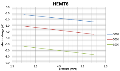
Fig.8.1. Electric charge on transistor HEMT6 at system without etching at different temperature
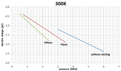
Fig.8.2. Electric charge on transistor HEMT6 at room temperature at different etching levels
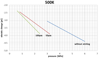
Fig.8.3.Electric charge on transistor HEMT6 at temperature 500K at different etching levels
Thermal expansion of materials affects the mechanical strain and thus the generated electric charge. This effect is illustrated on Fig.8.4. We see that the mechanical strain is positive on the whole model. This is due the fact that the material expands due to temperature. Strain at the location of transistor HEMT2, which was negative at room temperature has also changed to a positive value, resulting in the generation of negative charge on the electrode of this transistor.
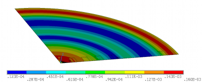
Fig.8.4. Mechanical strain in direction z at pressure 6MPa without etching at 500K
Fig.8.5. and Fig.8.6. show that the ambient temperature affects the sensitivity of the transistor HEMT2 and HEMT6. The sensitivity of these transistors has increased with the increasing temperature.
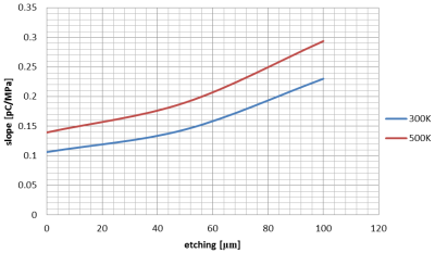
Fig.8.5. Dependence of HEMT2 transistor sensitivity on the etching level at different temperatures
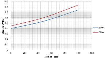
Fig.8.6. Dependence of HEMT6 transistor sensitivity on the etching level at different temperatures
9. Conclusion
This work describes the development of a piezoelectric pressure sensor model realized in the software Ansys. The aim was to create a 3D model physically similar to a real sensor. We obtained the character of the electric field intensity evaluated on the sensor´s surface. According to these data (Fig.6.2.), we can report the movement of the transistor HEMT2 towards the fixed region of the sensor, which increases the sensitivity. We investigated the differences in the electric charge on the gate electrodes of these transistors.
Results of the simulations showed that except of the transistor HEMT2 all transistors generated a negative electric charge. Negative electric charge has a depletion in the 2DEG channel, thus affects negatively the current flow in the structure. We are able obtain a more effective system if the sensor is loaded from the opposite direction, thus from the bottom of membrane. This type of loading results the creation of a positive charge on the transistors HEMT3, HEMT4, HEMT5 and HEMT6.
In the case of a positive charge the transistor HEMT6 indicated the highest sensitivity which is suitable for a pressure sensing system. The simulation of the etching procedure of the substrate material resulted an increasing sensitivity but also the maximum allowed pressure has decreased. Higher temperature changes affected the mechanical properties of the sensor, which is represented in the mechanical strain of the piezoelectric layer. This results the appearance of the negative electric charge on the gate electrodes.
References
- GAD-EL-HAK, M. The MEMS Handbook, MEMS-Design and fabrication,2006, vol.2
- AMBACHER, O. – SMART, J. – SHEALY, R. – WEIMANN, G. et al. Two dimensional electron hases induced by spontaneous and piezoelectric polarization charges in N- and Ga – face AlGaN/GaN heterostructures, Journal of applies physics, 1999,vol. 85, issue 6.
- PEARTON, S. – REN, F. – ZHANG, A. – LEE, K. Fabrication and performance of GaN electronic devices, Materials science and engineering , A review journal, 2000.
- JAVORKA, P. Fabrication and characterization of AlGaN/GaN high electron mobility transistors, 2004
- AMBACHER, O. Growth and applications of group III-nitrides. Journal of physics D: Applied physics. 2653-2710, 1998.
- AMBACHER, O. – SMART, J. – SHEALY, R. – WEIMANN, G. et al. Two dimensional electron gases induced by spontaneous and piezoelectric polarization charges in N- and Ga – face AlGaN/GaN heterostructures, Journalofappliesphysics,1999,vol. 85, issue 6.
- PEARTON, S. – REN, F. – ZHANG, A. – LEE, K. Fabrication and performance of GaN electronic devices, Materials science and engineering , A review journal, 2000.
- RUFER, L. – VITTOZ, S. – VANKO, G. – Lalinský, T. et al. AlGaN/GaN high electron mobility transistor based pressure sensor for harsh environments – Design and test, 2011.
- MUNRO, R. G. Material properties of a sinteredα-SiC, 1997, J. Phys. Chem. Ref. Data, Vol. 26, No. 5
- BARGHOUT, K. – CHAUDHURI, J. Calculation of residual thermal stress in GaN epitaxial layers grown on technologically important substrates, 2004.
- EDWARDS, M. Materials for robust gallium nitride – Temperature dependent properties of GaN, 2009
- VITANOV, S. – PALANKOVSKI,V. – Maroldt, S. – Quay,R. High-temperature modeling of AlGaN/GaN HEMTs, 2010
- PANDEY, D. K. – YADAV,R. R. Temperature dependent ultrasonic properties of aluminium nitride, 2008
- REEBER, R. R. – WANG, K. Lattice parameters and thermal expansion of important semiconductors and their substrates, 2000, vol. 622, Material research society
- Heraeus Quarzglas – Thermal properties, available online 20. 05. 2013
http://heraeus-quarzglas.com/en/quarzglas/thermalproperties/Thermal_properties.aspx - Advanced Energy Technology Group (Center of Energy Research) – Austentic stainless steel properties, available online 20. 05. 2013, http://aries.ucsd.edu/LIB/PROPS/PANOS/ss.html
- R. C. Turner, P. A. Fuierer, R. E. Newnham, T. R. Shrout, T. R., Appl. Acoust. 41 (1994) 299.
- M. AKIYAMA, T. KAMOHARA, K. NISHIKUBO, N. UENO, H. NAGAI, T. OKUTANI, Appl. Phys. Lett. 86 (2005) 02210
Coauthor of this paper are Ing. Gabriel Vanko PhD., doc. Ing. Vladimír Kutiš PhD, Institute of Power and Applied Electrical Engineering, Faculty of Electrical Engineering and Information Technology, Slovak University of Technology, Ilkovičova 3, Bratislava 84104, Slovakia

